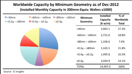
Over a quarter of industry wafer capacity dedicated to <40nm processes

Samsung, Intel, Toshiba/SanDisk had the greatest share of leading-edge capacity
More than a quarter of installed wafer capacity worldwide is dedicated to producing IC devices using process geometries (or feature sizes) smaller than 40nm, according to data in IC Insights' report, "Global Wafer Capacity 2013 - A Detailed Analysis and Forecast of the IC Industry's Wafer Fab Capacity".
The report also shows that a surprising amount of capacity remains dedicated to mature processes with "large" features sizes.
Installed capacity is divided into six categories based on the minimum geometry of the processes used in wafer fabrication.
The six categories range from <40nm; ≥40 - <60nm; ≥60nm - <80nm; ≥80nm - <0.2µ; ≥0.2µ - <0.4µ; ≥0.4µ. At the end of 2012, about 27 percent of global wafer capacity was for devices having geometries smaller than 40nm as shown in the figure at the top of this story.
Such devices include high-density DRAM, which are typically built using 30nm- to 20nm-class process technologies; high-density flash memory devices that are based on 20nm- to 10nm-class processes; and high-performance microprocessors and advanced ASIC/ASSP/FPGA devices based on 32/28nm or 22nm technologies.
About 22 percent of global capacity is dedicated to the ≥80nm - <0.2µ segment, which includes the 90nm, 0.13µ, and 0.18µ process generations. This "mature" process is widely used by pure-play foundries including TSMC, UMC, GlobalFoundries, SMIC, and TowerJazz and to manufacture a broad range of products for their diverse customer bases.
The least common technologies, at least in terms of the share of total installed capacity, are between the geometries of 80nm and 60nm (essentially the 65nm generation) and between 0.4µ and 0.2µ (essentially the 0.25µ and 0.35µ generations).
However, it is worth noting that the >0.4µ category maintains a fairly large share of total capacity, even though it has been longer than a decade-and-a-half since 0.5µ process technology was considered leading-edge.
The main reason is that huge quantities of commodity type devices such as standard analogue and general-purpose logic are manufactured with well-established process technologies having larger than 0.4µ feature sizes. In addition, high-voltage IC products require large-geometry process technologies.
Released in January 2013, the Global Wafer Capacity report assesses the IC industry's capacity by wafer size, minimum process geometry, technology type, geographic region, and by device type through 2017. The report also includes detailed profiles of the companies most likely to build 450mm wafer fabs and gives detailed specifications on existing wafer fab facilities.
Coupled with IC Insights' Strategic Reviews Online Database of more than 220 company profiles, the two reports provide a tremendous resource for researching, evaluating, and comparing wafer fab facilities and industry capacity.
The table below shows the leading suppliers of installed wafer capacity based on minimum geometry. It is not surprising that Samsung, Intel, Toshiba/SanDisk, SK Hynix, and Micron top the list with the greatest amount of leading-edge capacity. The biggest capacity holders in the large-feature process category (>0.2µ) consist of several analogue and mixed-signal chip suppliers.


